Done by Prof. Maurizio Gullo from University of Applied Sciences Northwestern Switzerland
Real-time movie captured from the 2PP 3D printer showing the fabrication process of a 3D cage structure. The structural filaments of both the cage and the integrated alignment marks are approximately 1 µm in thickness. As with other 2PP images, no scale bars are included in this visualization.
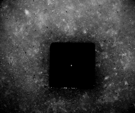
Snapshot from the two-photon polymerization (2PP) 3D printer utilizing backside illumination. The prominent black square (200 × 200 µm²) serves as the alignment mark. Centrally located is a silicon nitride (SiN) membrane containing a nanopore approximately 8–10 µm in diameter. Overlaid on this is a thinner, transparent polyethylene glycol diacrylate (PEGDA) membrane, approximately 2 µm thick, featuring a smaller pore with a diameter of ~0.8–1 µm. Note that scale bars are absent in these 2PP printer images.
Scanning electron microscope (SEM) image of the PEGDA membrane positioned within the engraved alignment square. The crater-like features observed in the bottom-left corner are artifacts caused by localized overheating or micro-explosions, likely resulting from impurities present during the laser-based 3D printing process.
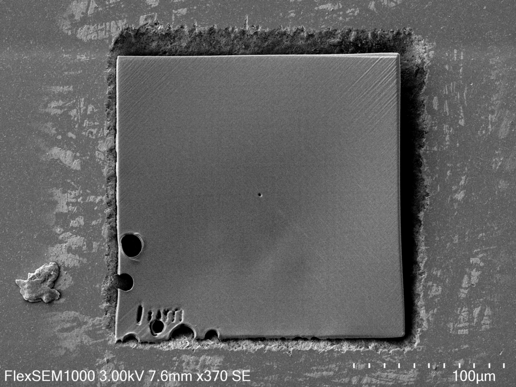
Zoomed-in SEM image of the membrane aperture shown in Figure 2, highlighting the smaller pore of ~0.8–1 µm in diameter. While the outer diameter of the aperture matches the original design specifications, the inner diameter is typically reduced by 20–30% due to proximity effects and diffusion limitations during the development stage of the fabrication process.
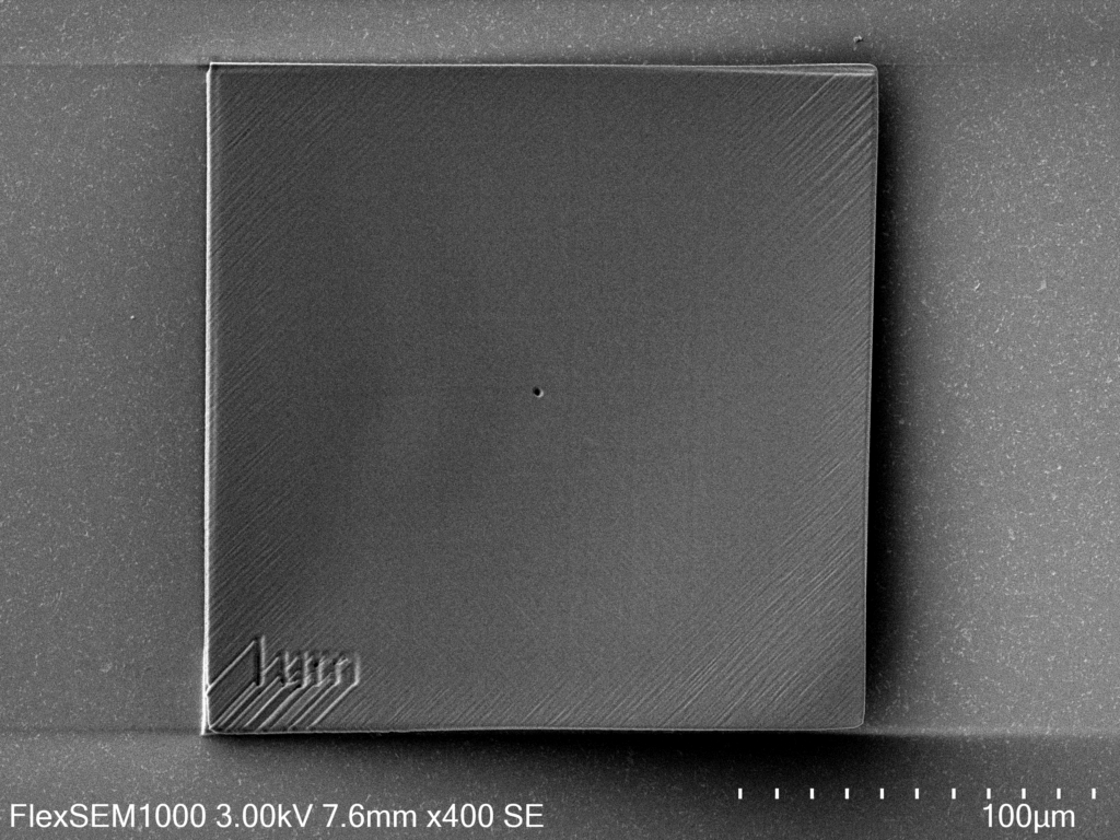
SEM image of a PEGDA membrane fabricated on the flat side of the chip, illustrating a defect-free structure. No signs of thermal damage or material degradation due to laser-induced overheating are visible in this configuration.